公告版位
Bewise Inc. www.tool-tool.com Reference source from the internet.

The Magdeburg hemispheres were a pair of large copper hemispheres with mating rims. When the rims were sealed with grease and the air was pumped out, the sphere contained a vacuum and could not be pulled apart by teams of horses. The Magdeburg hemispheres were designed by German scientist Otto von Guericke in 1650 to demonstrate the air pump he had invented and the concept of air pressure. The first artificial vacuum had been produced a few years earlier by Evangelista Torricelli, and had inspired von Guericke to design the world's first vacuum pump, which consisted of a piston and cylinder with one-way flap valves. To power the machine, several people would turn a crank arm connected to the vacuum pump.

Gaspar Schott's sketch of Otto von Guericke's Magdeburg hemispheres experiment.

Contents

[hide]

[edit] Overview

The Magdeburg hemispheres, a little over a foot (30 cm) in diameter, were designed to demonstrate the vacuum pump that von Guericke had invented. When the air was sucked out from inside them, they were held firmly together by the air pressure of the surrounding atmosphere.

[edit] Demonstrations

Guericke's demonstration was presented on 8 May 1654 to the Reichstag and the Emperor Ferdinand III in 1654 in Regensburg, where 30 horses, in two teams of 15, could not separate the hemispheres until the vacuum was released. In 1656 he repeated the demonstration with 16 horses (2 teams of 8) in his hometown of Magdeburg, where he was mayor. In 1657, Gaspar Schott was the first to describe the experiment in print in his Mechanica Hydraulico-Pneumatica. In 1663 (or according to some sources in 1661) the demonstration was given in Berlin before Frederick William, Elector of Brandenburg) with 24 horses.

The original hemispheres are maintained by the Deutsches Museum in Munich. Many copies of them (usually smaller) have been made to illustrate the principle of air pressure to students. Re-enactments of von Guerike's 1654 experiment are performed in locations around the world by the Otto von Guericke Society. The experiment has been commemorated on at least two German stamps.

[edit] Related

After learning about Guericke's pump through Schott's book, Robert Boyle worked with Robert Hooke to design and build an improved air pump. From this, through various experiments, they formulated what is called Boyle's law, which states that the volume of a body of an ideal gas is inversely proportional to its pressure. Soon the ideal gas law was formulated.

Based on these concepts, in 1679, an associate of Boyle's named Denis Papin built a bone digester, which is a closed vessel with a tightly fitting lid that confines steam until a high pressure is generated. Later designs implemented a steam release valve to keep the machine from exploding. By watching the valve rhythmically move up and down, Papin conceived of the idea of a piston and cylinder engine. He did not, however, follow through with his design. Nevertheless, in 1697, based on Papin's designs, engineer Thomas Savery built the first commercial steam engine.

歡迎來到Bewise Inc.的世界,首先恭喜您來到這接受新的資訊讓產業更有競爭力,我們是提供專業刀具製造商,應對客戶高品質的刀具需求,我們可以協助客戶滿足您對產業的不同要求,我們有能力達到非常卓越的客戶需求品質,這是現有相關技術無法比擬的,我們成功的滿足了各行各業的要求,包括:精密HSS DIN切削刀具協助客戶設計刀具流程DIN or JIS 鎢鋼切削刀具設計NAS986 NAS965 NAS897 NAS937orNAS907 航太切削刀具,NAS航太刀具設計超高硬度的切削刀具BW捨棄式鑽石V卡刀BW捨棄式金屬圓鋸片木工捨棄式金屬圓鋸片PCD木工圓鋸片醫療配件刀具設計汽車業刀具設計電子產業鑽石刀具全鎢鋼V卡刀-電路版專用全鎢鋼鋸片焊刃式側銑刀焊刃式千鳥側銑刀焊刃式T型銑刀焊刃式千鳥T型銑刀焊刃式螺旋機械鉸刀全鎢鋼斜邊刀電路版專用鎢鋼焊刃式高速鉸刀超微粒鎢鋼機械鉸刀超微粒鎢鋼定點鑽焊刃式帶柄角度銑刀焊刃式螺旋立銑刀焊刃式帶柄倒角銑刀焊刃式角度銑刀焊刃式筒型平面銑刀木工產業鑽石刀具等等。我們的產品涵蓋了從民生刀具到工業級的刀具設計;從微細刀具到大型刀具;從小型生產到大型量產;全自動整合;我們的技術可提供您連續生產的效能,我們整體的服務及卓越的技術,恭迎您親自體驗!!

BW Bewise Inc. Willy Chen willy@tool-tool.com bw@tool-tool.com www.tool-tool.com skype:willy_chen_bw mobile:0937-618-190 Head &Administration Office No.13,Shiang Shang 2nd St., West Chiu Taichung,Taiwan 40356 http://www.tool-tool..com / FAX:+886 4 2471 4839 N.Branch 5F,No.460,Fu Shin North Rd.,Taipei,Taiwan S.Branch No.24,Sec.1,Chia Pu East Rd.,Taipao City,Chiayi Hsien,Taiwan

Welcome to BW tool world! We are an experienced tool maker specialized in cutting tools. We focus on what you need and endeavor to research the best cutter to satisfy users demand. Our customers involve wide range of industries, like mold & die, aerospace, electronic, machinery, etc. We are professional expert in cutting field. We would like to solve every problem from you. Please feel free to contact us, its our pleasure to serve for you. BW product including: cutting toolaerospace tool .HSS DIN Cutting toolCarbide end millsCarbide cutting toolNAS Cutting toolNAS986 NAS965 NAS897 NAS937orNAS907 Cutting Tools,Carbide end milldisc milling cutter,Aerospace cutting toolhss drillФрезерыCarbide drillHigh speed steelMilling cutterCVDD(Chemical Vapor Deposition Diamond )’PCBN (Polycrystalline Cubic Boron Nitride) Core drillTapered end millsCVD Diamond Tools Inserts’PCD Edge-Beveling Cutter(Golden FingerEdge modifying knifeSolid carbide saw blade-V typeV-type locking-special use for PC boardMetal Slitting SawaCarbide Side milling CuttersCarbide Side Milling Cutters With Staggered TeethCarbide T-Slot Milling CuttersCarbide T-Slot Milling Cutters With Staggered TeethCarbide Machine ReamersHigh speed reamer-standard typeHigh speed reamer-long type’’PCD V-CutterPCD Wood toolsPCD Cutting toolsPCD Circular Saw BladePVDD End Millsdiamond tool V-type locking-special use for PC board Single Crystal Diamond Metric end millsMiniature end millsСпециальные режущие инструменты Пустотелое сверло Pilot reamerFraisesFresas con mango PCD (Polycrystalline diamond) ‘FreseElectronics cutterStep drillMetal cutting sawDouble margin drillGun barrelAngle milling cutterCarbide burrsCarbide tipped cutterChamfering toolIC card engraving cutterSide cutterNAS toolDIN or JIS toolSpecial toolMetal slitting sawsShell end millsSide and face milling cuttersSide chip clearance sawsLong end millsStub roughing end millsDovetail milling cuttersCarbide slot drillsCarbide torus cuttersAngel carbide end millsCarbide torus cuttersCarbide ball-nosed slot drillsMould cutterTool manufacturer.

Bewise Inc. www.tool-tool.com

ようこそBewise Inc.の世界へお越し下さいませ、先ず御目出度たいのは新たな

情報を受け取って頂き、もっと各産業に競争力プラス展開。

弊社は専門なエンドミルの製造メーカーで、客先に色んな分野のニーズ

豊富なパリエーションを満足させ、特にハイテク品質要求にサポート致します。

弊社は各領域に供給できる内容は:</</body>

beeway 發表在 痞客邦 留言(0) 人氣()

Bewise Inc. www.tool-tool.com Reference source from the internet.

A field emission display (FED) is a type of flat panel display using field emitting cathodes to bombard phosphor coatings as the light emissive medium.

Field emission displays are very similar to cathode ray tubes, however they are only a few millimeters thick. Instead of a single electron gun, a field emission display (FED) uses a large array of fine metal tips or carbon nanotubes (which are the most efficient electron emitters known), with many positioned behind each phosphor dot, to emit electrons through a process known as field emission. Because of emitter redundancy, FEDs do not display dead pixels like LCDs even if 20% of the emitters fail. Sony is researching FED because it is the flat-panel technology that comes closest to matching the picture of a CRT.[citation needed]

FEDs are energy efficient and could provide a flat panel technology that features less power consumption than existing LCD and plasma display technologies. They can also be cheaper to make, as they have fewer total components. As of yet, however, there are no consumer production models available in the United States, although small demo panels have been produced.

A similar technology to be commercialized in 2007 is the SED (surface-conduction electron-emitter) display, a simplified variant of FED technology. Whereas FED uses a 'Spindt tip' semi-conductor or carbon nanotube emitter, with multiple redundant emitters per area of display[1], SED uses a single emitter based on palladium oxide laid down by an inkjet or silk-screen process.[2]. SED is considered the variant of FED that is currently feasible to mass-produce.

In 2001, Candescent had spent $600 million on producing FEDs with non-carbon material, but it was abandoned, with assets sold to Canon in August 2004, two months after filing for voluntary reorganization under Chapter 11. The UK company Advance Nanotech, in collaboration with the University of Bristol, has developed a similar panel that relies on specially doped diamond dust. The first 1000 Carbon Nanotechnologies was set to production in late 2006 by Sony. [3]

Nano-emissive display is the name given by Motorola for field emission display. A prototype model was demonstrated by Motorola in May 2005. Nano-emissive display (NED) is Motorola's term for their Carbon Nanotubes (CNTs)-based display technology.

Contents

[hide]

[edit] Potential disadvantages

Although physically simple, actual operation of field emitters in a production device are anything but simple. Field emitters depend on high electric field strength to tear electrons from the surface. Instead of very high voltages, FEDs use very small radii – atomic lattice size – and element spacing for cathodes. This small size renders the cathodes susceptible to damage by ion impact. The ions are produced by the high voltages interacting with residual gas molecules inside the device. FEDs require high vacuum levels which are difficult to attain: the vacuum suitable for conventional CRTs and vacuum tubes is not sufficient for long term FED operation. Intense electron bombardment of the phosphor layer will also release gas during use.

歡迎來到Bewise Inc.的世界,首先恭喜您來到這接受新的資訊讓產業更有競爭力,我們是提供專業刀具製造商,應對客戶高品質的刀具需求,我們可以協助客戶滿足您對產業的不同要求,我們有能力達到非常卓越的客戶需求品質,這是現有相關技術無法比擬的,我們成功的滿足了各行各業的要求,包括:精密HSS DIN切削刀具協助客戶設計刀具流程DIN or JIS 鎢鋼切削刀具設計NAS986 NAS965 NAS897 NAS937orNAS907 航太切削刀具,NAS航太刀具設計超高硬度的切削刀具BW捨棄式鑽石V卡刀BW捨棄式金屬圓鋸片木工捨棄式金屬圓鋸片PCD木工圓鋸片醫療配件刀具設計汽車業刀具設計電子產業鑽石刀具全鎢鋼V卡刀-電路版專用全鎢鋼鋸片焊刃式側銑刀焊刃式千鳥側銑刀焊刃式T型銑刀焊刃式千鳥T型銑刀焊刃式螺旋機械鉸刀全鎢鋼斜邊刀電路版專用鎢鋼焊刃式高速鉸刀超微粒鎢鋼機械鉸刀超微粒鎢鋼定點鑽焊刃式帶柄角度銑刀焊刃式螺旋立銑刀焊刃式帶柄倒角銑刀焊刃式角度銑刀焊刃式筒型平面銑刀木工產業鑽石刀具等等。我們的產品涵蓋了從民生刀具到工業級的刀具設計;從微細刀具到大型刀具;從小型生產到大型量產;全自動整合;我們的技術可提供您連續生產的效能,我們整體的服務及卓越的技術,恭迎您親自體驗!!

BW Bewise Inc. Willy Chen willy@tool-tool.com bw@tool-tool.com www.tool-tool.com skype:willy_chen_bw mobile:0937-618-190 Head &Administration Office No.13,Shiang Shang 2nd St., West Chiu Taichung,Taiwan 40356 http://www.tool-tool..com / FAX:+886 4 2471 4839 N.Branch 5F,No.460,Fu Shin North Rd.,Taipei,Taiwan S.Branch No.24,Sec.1,Chia Pu East Rd.,Taipao City,Chiayi Hsien,Taiwan

Welcome to BW tool world! We are an experienced tool maker specialized in cutting tools. We focus on what you need and endeavor to research the best cutter to satisfy users demand. Our customers involve wide range of industries, like mold & die, aerospace, electronic, machinery, etc. We are professional expert in cutting field. We would like to solve every problem from you. Please feel free to contact us, its our pleasure to serve for you. BW product including: cutting toolaerospace tool .HSS DIN Cutting toolCarbide end millsCarbide cutting toolNAS Cutting toolNAS986 NAS965 NAS897 NAS937orNAS907 Cutting Tools,Carbide end milldisc milling cutter,Aerospace cutting toolhss drillФрезерыCarbide drillHigh speed steelMilling cutterCVDD(Chemical Vapor Deposition Diamond )’PCBN (Polycrystalline Cubic Boron Nitride) Core drillTapered end millsCVD Diamond Tools Inserts’PCD Edge-Beveling Cutter(Golden FingerEdge modifying knifeSolid carbide saw blade-V typeV-type locking-special use for PC boardMetal Slitting SawaCarbide Side milling CuttersCarbide Side Milling Cutters With Staggered TeethCarbide T-Slot Milling CuttersCarbide T-Slot Milling Cutters With Staggered TeethCarbide Machine ReamersHigh speed reamer-standard typeHigh speed reamer-long type’’PCD V-CutterPCD Wood toolsPCD Cutting toolsPCD Circular Saw BladePVDD End Millsdiamond tool V-type locking-special use for PC board Single Crystal Diamond Metric end millsMiniature end millsСпециальные режущие инструменты Пустотелое сверло Pilot reamerFraisesFresas con mango PCD (Polycrystalline diamond) ‘FreseElectronics cutterStep drillMetal cutting sawDouble margin drillGun barrelAngle milling cutterCarbide burrsCarbide tipped cutterChamfering toolIC card engraving cutterSide cutterNAS toolDIN or JIS toolSpecial toolMetal slitting sawsShell end millsSide and face milling cuttersSide chip clearance sawsLong end millsStub roughing end millsDovetail milling cuttersCarbide slot drillsCarbide torus cuttersAngel carbide end millsCarbide torus cuttersCarbide ball-nosed slot drillsMould cutterTool manufacturer.

Bewise Inc. www.tool-tool.com

ようこそBewise Inc.の世界へお越し下さいませ、先ず御目出度たいのは新たな

情報を受け取って頂き、もっと各産業に競争力プラス展開。

弊社は専門なエンドミルの製造メーカーで、客先に色んな分野のニーズ

豊富なパリエーションを満足させ、特にハイテク品質要求にサポート致します。

弊社は各領域に供給できる内容は:

(1)精密HSSエンドミルのR&D

(2)Carbide Cutting tools設計

beeway 發表在 痞客邦 留言(0) 人氣()

Bewise Inc. www.tool-tool.com Reference source from the internet.
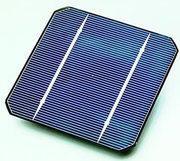
A solar cell, made from a monocrystalline silicon wafer

A solar cell, made from a monocrystalline silicon wafer

A solar cell or photovoltaic cell is a device that converts solar energy into electricity by the photovoltaic effect. Photovoltaics is the field of technology and research related to the application of solar cells as solar energy. Sometimes the term solar cell is reserved for devices intended specifically to capture energy from sunlight, while the term photovoltaic cell is used when the source is unspecified.

Assemblies of cells are used to make solar modules, which may in turn be linked in photovoltaic arrays.

Solar cells have many applications. Individual cells are used for powering small devices such as electronic calculators. Photovoltaic arrays generate a form of renewable electricity, particularly useful in situations where electrical power from the grid is unavailable such as in remote area power systems, Earth-orbiting satellites and space probes, remote radiotelephones and water pumping applications. Photovoltaic electricity is also increasingly deployed in grid-tied electrical systems.

[edit] History

The term "photovoltaic" comes from the Greek φώς:phos meaning "light", and "voltaic", meaning electrical, from the name of the Italian physicist Volta, after whom the measurement unit volt is named. The term "photo-voltaic" has been in use in English since 1849.[1]

The photovoltaic effect was first recognized in 1839 by French physicist Alexandre-Edmond Becquerel. However, it was not until 1883 that the first solar cell was built, by Charles Fritts, who coated the semiconductor selenium with an extremely thin layer of gold to form the junctions. The device was only around 1% efficient. Russell Ohl patented the modern solar cell in 1946 (U.S. Patent 2,402,662 , "Light sensitive device"). Sven Ason Berglund had a prior patent concerning methods of increasing the capacity of photosensitive cells. The modern age of solar power technology arrived in 1954 when Bell Laboratories, experimenting with semiconductors, accidentally found that silicon doped with certain impurities was very sensitive to light.

This resulted in the production of the first practical solar cells with a sunlight energy conversion efficiency of around 6 percent. Russia launched the first artificial satellite in 1957, and the United States' first artificial satellite was launched in 1958 using solar cells created by Peter Iles in an effort spearheaded by Hoffman Electronics. The first spacecraft to use solar panels was the US satellite Explorer 1 in January 1958. This milestone created interest in producing and launching a geostationary communications satellite, in which solar energy would provide a viable power supply. This was a crucial development which stimulated funding from several governments into research for improved solar cells.

In 1970 the first highly effective GaAs heterostructure solar cells were created by Zhores Alferov and his team in the USSR. [2][3][4] Metal Organic Chemical Vapor Deposition (MOCVD, or OMCVD) production equipment was not developed until the early 1980s, limiting the ability of companies to manufacture the GaAs solar cell. In the United States, the first 17% efficient air mass zero (AM0) single-junction GaAs solar cells were manufactured in production quantities in 1988 by Applied Solar Energy Corporation (ASEC). The "dual junction" cell was accidentally produced in quantity by ASEC in 1989 as a result of the change from GaAs on GaAs substrates to GaAs on Germanium (Ge) substrates. The accidental doping of Ge with the GaAs buffer layer created higher open circuit voltages, demonstrating the potential of using the Ge substrate as another cell. As GaAs single-junction cells topped 19% AM0 production efficiency in 1993, ASEC developed the first dual junction cells for spacecraft use in the United States, with a starting efficiency of approximately 20%. These cells did not utilize the Ge as a second cell, but used another GaAs-based cell with different doping. Eventually GaAs dual junction cells reached production efficiencies of about 22%. Triple Junction solar cells began with AM0 efficiencies of approximately 24% in 2000, 26% in 2002, 28% in 2005, and in 2007 have evolved to a 30% AM0 production efficiency, currently in qualification. In 2007, two companies in the United States, Emcore Photovoltaics and Spectrolab, produce 95% of the world's 28% efficient solar cells.

Possible reference please confirm. Retrieved on 2008-05-22.

The first generation photovoltaic cell consists of a large-area, single-crystal, single layer p-n junction diode, capable of generating usable electrical energy from light sources with the wavelengths of sunlight. These cells are typically made using a diffusion process with silicon wafers. First-generation photovoltaic cells (also known as silicon wafer-based solar cells) are the dominant technology in the commercial production of solar cells, accounting for more than 86% of the terrestrial solar cell market.

The second generation of photovoltaic materials is based on the use of thin epitaxial deposits of semiconductors on lattice-matched wafers. There are two classes of epitaxial photovoltaics - space and terrestrial. Space cells typically have higher AM0 efficiencies (28-30%) in production, but have a higher cost per watt. Their "thin-film" cousins have been developed using lower-cost processes, but have lower AM0 efficiencies (7-9%) in production and are questionable for space applications. The advent of thin-film technology contributed to a prediction of greatly reduced costs for thin film solar cells that has yet to be achieved. There are currently (2007) a number of technologies/semiconductor materials under investigation or in mass production. Examples include amorphous silicon, polycrystalline silicon, micro-crystalline silicon, cadmium telluride, copper indium selenide/sulfide. An advantage of thin-film technology theoretically results in reduced mass so it allows fitting panels on light or flexible materials, even textiles. The advent of thin GaAs-based films for space applications (so-called "thin cells") with potential AM0 efficiencies of up to 37% are currently in the development stage for high specific power applications. Second generation solar cells now comprise a small segment of the terrestrial photovoltaic market, and approximately 90% of the space market.

Third-generation photovoltaics are proposed to be very different from the previous semiconductor devices as they do not rely on a traditional p-n junction to separate photogenerated charge carriers. For space applications quantum well devices (quantum dots, quantum ropes, etc.) and devices incorporating carbon nanotubes are being studied - with a potential for up to 45% AM0 production efficiency. For terrestrial applications, these new devices include photoelectrochemical cells, polymer solar cells, nanocrystal solar cells, Dye-sensitized solar cells and are still in the research phase.

[edit] Applications and implementations
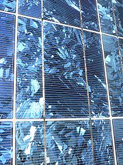
Polycrystaline PV cells laminated to backing material in a PV module

Polycrystaline PV cells laminated to backing material in a PV module
Polycrystalline PV cells

Polycrystalline PV cells
Main article: photovoltaic array

Solar cells are often electrically connected and encapsulated as a module. PV modules often have a sheet of glass on the front (sun up) side , allowing light to pass while protecting the semiconductor wafers from the elements (rain, hail, etc.). Solar cells are also usually connected in series in modules, creating an additive voltage. Connecting cells in parallel will yield a higher current. Modules are then interconnected, in series or parallel, or both, to create an array with the desired peak DC voltage and current.

The power output of a solar array is measured in watts or kilowatts. In order to calculate the typical energy needs of the application, a measurement in watt-hours, kilowatt-hours or kilowatt-hours per day is often used. A common rule of thumb is that average power is equal to 20% of peak power, so that each peak kilowatt of solar array output power corresponds to energy production of 4.8 kW·h per day.

To make practical use of the solar-generated energy, the electricity is most often fed into the electricity grid using inverters (grid-connected PV systems); in stand alone systems, batteries are used to store the energy that is not needed immediately.

[edit] Theory

[edit] Simple explanation

  1. Photons in sunlight hit the solar panel and are absorbed by semiconducting materials, such as silicon.
  2. Electrons (negatively charged) are knocked loose from their atoms, allowing them to flow through the material to produce electricity. The complementary positive charges that are also created (like bubbles) are called holes and flow in the direction opposite of the electrons in a silicon solar panel.
  3. An array of solar panels converts solar energy into a usable amount of direct current (DC) electricity.

Optionally:

  1. The DC current enters an inverter.
  2. The inverter turns DC electricity into 120 or 240-volt AC (alternating current) electricity needed for home appliances.
  3. The AC power enters the utility panel in the house.
  4. The electricity is then distributed to appliances or lights in the house.
  5. The electricity that is not used will be re-routed and used in other facilities.

[edit] Photogeneration of charge carriers

When a photon hits a piece of silicon, one of three things can happen:

  1. the photon can pass straight through the silicon — this (generally) happens for lower energy photons,
  2. the photon can reflect off the surface,
  3. the photon can be absorbed by the silicon, if the photon energy is higher than the silicon band gap value. This generates an electron-hole pair and sometimes heat, depending on the band structure.

When a photon is absorbed, its energy is given to an electron in the crystal lattice. Usually this electron is in the valence band, and is tightly bound in covalent bonds between neighboring atoms, and hence unable to move far. The energy given to it by the photon "excites" it into the conduction band, where it is free to move around within the semiconductor. The covalent bond that the electron was previously a part of now has one fewer electron — this is known as a hole. The presence of a missing covalent bond allows the bonded electrons of neighboring atoms to move into the "hole," leaving another hole behind, and in this way a hole can move through the lattice. Thus, it can be said that photons absorbed in the semiconductor create mobile electron-hole pairs.

A photon need only have greater energy than that of the band gap in order to excite an electron from the valence band into the conduction band. However, the solar frequency spectrum approximates a black body spectrum at ~6000 K, and as such, much of the solar radiation reaching the Earth is composed of photons with energies greater than the band gap of silicon. These higher energy photons will be absorbed by the solar cell, but the difference in energy between these photons and the silicon band gap is converted into heat (via lattice vibrations — called phonons) rather than into usable electrical energy.

[edit] Charge carrier separation

There are two main modes for charge carrier separation in a solar cell:

  1. drift of carriers, driven by an electrostatic field established across the device
  2. diffusion of carriers from zones of high carrier concentration to zones of low carrier concentration (following a gradient of electrochemical potential).

In the widely used p-n junction solar cells, the dominant mode of charge carrier separation is by drift. However, in non-p-n-junction solar cells (typical of the third generation of solar cell research such as dye and polymer thin-film solar cells), a general electrostatic field has been confirmed to be absent, and the dominant mode of separation is via charge carrier diffusion.[citation needed]

[edit] The p-n junction

Main article: semiconductor

The most commonly known solar cell is configured as a large-area p-n junction made from silicon. As a simplification, one can imagine bringing a layer of n-type silicon into direct contact with a layer of p-type silicon. In practice, p-n junctions of silicon solar cells are not made in this way, but rather, by diffusing an n-type dopant into one side of a p-type wafer (or vice versa).

If a piece of p-type silicon is placed in intimate contact with a piece of n-type silicon, then a diffusion of electrons occurs from the region of high electron concentration (the n-type side of the junction) into the region of low electron concentration (p-type side of the junction). When the electrons diffuse across the p-n junction, they recombine with holes on the p-type side. The diffusion of carriers does not happen indefinitely however, because of an electric field which is created by the imbalance of charge immediately on either side of the junction which this diffusion creates. The electric field established across the p-n junction creates a diode that promotes current to flow in only one direction across the junction. Electrons may pass from the p-type side into the n-type side, and holes may pass from the n-type side to the p-type side, but not the other way around[5]. This region where electrons have diffused across the junction is called the depletion region because it no longer contains any mobile charge carriers. It is also known as the "space charge region".

[edit] Connection to an external load

Ohmic metal-semiconductor contacts are made to both the n-type and p-type sides of the solar cell, and the electrodes connected to an external load. Electrons that are created on the n-type side, or have been "collected" by the junction and swept onto the n-type side, may travel through the wire, power the load, and continue through the wire until they reach the p-type semiconductor-metal contact. Here, they recombine with a hole that was either created as an electron-hole pair on the p-type side of the solar cell, or swept across the junction from the n-type side after being created there.

[edit] Equivalent circuit of a solar cell
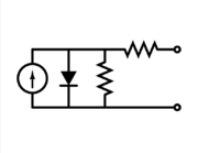
The equivalent circuit of a solar cell

The equivalent circuit of a solar cell
The schematic symbol of a solar cell

The schematic symbol of a solar cell

To understand the electronic behavior of a solar cell, it is useful to create a model which is electrically equivalent, and is based on discrete electrical components whose behavior is well known. An ideal solar cell may be modelled by a current source in parallel with a diode; in practice no solar cell is ideal, so a shunt resistance and a series resistance component are added to the model.[6] The resulting equivalent circuit of a solar cell is shown on the left. Also shown, on the right, is the schematic representation of a solar cell for use in circuit diagrams.

[edit] Circuit Equations defining solar cell

The equations which describe the I-V characteristics of the cell are

  1. I = I_L - I_o \left( e^{q \left( V + I \times R_s \right) / nkT} - 1 \right)
  2. I_L = I_{L \left( T_1 \right)} \left( 1 + K_o \left(T - T_1 \right) \right)
  3. I_{L \left( T_1 \right)} = G \times I_{sc \left( T_1 \right) }
  4. K_o = \left( I_{ sc \left(T_2 \right) } - I_{sc \left( T_1 \right) } \right) / \left( T_2 - T_1 \right)
  5. I_o = I_{ o \left( T_1 \right) } \times {\left( T / T_1 \right)}^{3/n} * e^{ -q * V_g / nk * \left( 1/T - 1/T_1 \right)}
  6. I_{ o \left( T_1 \right) } = I_{ sc \left( T_1 \right) }/ \left( e^{ q*V_{ oc \left( T_1 \right) } / nkT_1 } - 1 \right)
  7. R_s = - { \left( \tfrac{dV}{dI} \right) }_{ V_{oc} } - 1 / X_v
  8. X_v = I_{ o \left( T_1 \right) } \times q / nkT_1 \times e^{ q*V_{ oc \left( T_1 \right) } / nkT_1 }

where

  • k is Boltzman's constant
  • q is charge on an electron
  • Vg is band gap voltage
  • n is diode quality factor
  • Rs is series resistance of cell
  • Rsh is shunt resistance
  • T1 and T2 are reference temperature in Kelvin
  • T is working temperature of cell in Kelvin
  • Voc is open circuit voltage
  • Isc is short circuit current
  • Io is reverse saturation current of diode
  • I is the current through Rs
  • IL is current produced by the cell

in many sources IL is also known as Iph.

[edit] Solar cell efficiency factors

[edit] Energy conversion efficiency

A solar cell's energy conversion efficiency (η, "eta"), is the percentage of power converted (from absorbed light to electrical energy) and collected, when a solar cell is connected to an electrical circuit. This term is calculated using the ratio of the maximum power point, Pm, divided by the input light irradiance (E, in W/m²) under standard test conditions (STC) and the surface area of the solar cell (Ac in m²).

\eta = \frac{P_{m}}{E \times A_c}

STC specifies a temperature of 25°C and an irradiance of 1000 W/m² with an air mass 1.5 (AM1.5) spectrum. These correspond to the irradiance and spectrum of sunlight incident on a clear day upon a sun-facing 37°-tilted surface with the sun at an angle of 41.81° above the horizon.[7][8] This condition approximately represents solar noon near the spring and autumn equinoxes in the continental United States with surface of the cell aimed directly at the sun. Thus, under these conditions a solar cell of 12% efficiency with a 100 cm2 (0.01 m2) surface area can be expected to produce approximately 1.2 watts of power.

The losses of a solar cell may be broken down into reflectance losses, thermodynamic efficiency, recombination losses and resistive electrical loss. The overall efficiency is the product of each of these individual losses.

Due to the difficulty in measuring these parameters directly, other parameters are measured instead: Thermodynamic Efficiency, Quantum Efficiency, VOC ratio, and Fill Factor. Reflectance losses are a portion of the Quantum Efficiency under "External Quantum Efficiency". Recombination losses make up a portion of the Quantum Efficiency, VOC ratio, and Fill Factor. Resistive losses are predominantly categorized under Fill Factor, but also make up minor portions of the Quantum Efficiency, VOC ratio.

[edit] Thermodynamic Efficiency Limit

Solar cells operate as quantum energy conversion devices, and are therefore subject to the "Thermodynamic Efficiency Limit". Photons with an energy below the band gap of the absorber material cannot generate a hole-electron pair, and so their energy is not converted to useful output and only generates heat if absorbed. For photons with an energy above the band gap energy, only a fraction of the energy above the band gap can be converted to useful output. When a photon of greater energy is absorbed, the excess energy above the band gap is converted to kinetic energy of the carrier combination. The excess kinetic energy is converted to heat through phonon interactions as the kinetic energy of the carriers slows to equilibrium velocity.

Solar cells with multiple band gap absorber materials are able to more efficiently convert the solar spectrum. By using multiple band gaps, the solar spectrum may be broken down into smaller bins where the thermodynamic efficiency limit is higher for each bin.[9]

[edit] Quantum efficiency

As described above, when a photon is absorbed by a solar cell it is converted to an electron-hole pair. This electron-hole pair may then travel to the surface of the solar cell and contribute to the current produced by the cell; such a carrier is said to be collected. Alternatively, the carrier may give up its energy and once again become bound to an atom within the solar cell without reaching the surface; this is called recombination, and carriers that recombine do not contribute to the production of electrical current.

Quantum efficiency refers to the percentage of photons that are converted to electric current (i.e., collected carriers) when the cell is operated under short circuit conditions. External quantum efficiency is the fraction of incident photons that are converted to electrical current, while internal quantum efficiency is the fraction of absorbed photons that are converted to electrical current. Mathematically, internal quantum efficiency is related to external quantum efficiency by the reflectance of the solar cell; given a perfect anti-reflection coating, they are the same.

Quantum efficiency should not be confused with energy conversion efficiency, as it does not convey information about the power collected from the solar cell. Furthermore, quantum efficiency is most usefully expressed as a spectral measurement (that is, as a function of photon wavelength or energy). Since some wavelengths are absorbed more effectively than others in most semiconductors, spectral measurements of quantum efficiency can yield information about which parts of a particular solar cell design are most in need of improvement.

[edit] VOC ratio

Due to recombination, the open circuit voltage (VOC) of the cell will be below the band gap voltage of the cell. Since the energy of the photons must be at or above the band gap to generate a carrier pair, cell voltage below the band gap voltage represents a loss. This loss is represented by the ratio of VOC divided by VG

[edit] Maximum-power point

A solar cell may operate over a wide range of voltages (V) and currents (I). By increasing the resistive load on an irradiated cell continuously from zero (a short circuit) to a very high value (an open circuit) one can determine the maximum-power point, the point that maximizes V×I; that is, the load for which the cell can deliver maximum electrical power at that level of irradiation. (The output power is zero in both the short circuit and open circuit extremes).

A high quality, monocrystalline silicon solar cell, at 25 °C cell temperature, may produce 0.60 volts open-circuit (Voc). The cell temperature in full sunlight, even with 25 °C air temperature, will probably be close to 45 °C, reducing the open-circuit voltage to 0.55 volts per cell. The voltage drops modestly, with this type of cell, until the short-circuit current is approached (Isc). Maximum power (with 45 °C cell temperature) is typically produced with 75% to 80% of the open-circuit voltage (0.43 volts in this case) and 90% of the short-circuit current. This output can be up to 70% of the Voc x Isc product. The short-circuit current (Isc) from a cell is nearly proportional to the illumination, while the open-circuit voltage (Voc) may drop only 10% with a 80% drop in illumination. Lower-quality cells have a more rapid drop in voltage with increasing current and could produce only 1/2 Voc at 1/2 Isc. The usable power output could thus drop from 70% of the Voc x Isc product to 50% or even as little as 25%. Vendors who rate their solar cell "power" only as Voc x Isc, without giving load curves, can be seriously distorting their actual performance.

The maximum power point of a photovoltaic varies with incident illumination. For systems large enough to justify the extra expense, a maximum power point tracker tracks the instantaneous power by continually measuring the voltage and current (and hence, power transfer), and uses this information to dynamically adjust the load so the maximum power is always transferred, regardless of the variation in lighting.

[edit] Fill factor

Another defining term in the overall behavior of a solar cell is the fill factor (FF). This is the ratio of the maximum power point divided by the open circuit voltage (Voc) and the short circuit current (Isc):

FF = \frac{P_{m}}{V_{oc} \times I_{sc}} = \frac{\eta \times A_c \times E}{V_{oc} \times I_{sc}}

[edit] Comparison of energy conversion efficiencies

Main article: Photovoltaics

At this point, discussion of the different ways to calculate efficiency for space cells and terrestrial cells is necessary to alleviate confusion. In space, where there is no atmosphere, the spectrum of the sun is relatively unfiltered. However on earth, with air filtering the incoming light, the solar spectrum changes. To account for the spectral differences, a system was devised to calculate this filtering effect. Simply, the filtering effect ranges from Air Mass 0 in space, to approximately Air Mass 1.5 on earth. Multiplying the spectral differences by the quantum efficiency of the solar cell in question will yield the efficiency of the device. For example, a Silicon solar cell in space might have an efficiency of 14% at AM0, but have an efficiency of 16% on earth at AM 1.5. Terrestrial efficiencies typically are greater than space efficiencies.

Solar cell efficiencies vary from 6% for amorphous silicon-based solar cells to 40.7% with multiple-junction research lab cells and 42.8% with multiple dies assembled into a hybrid package.[10] Solar cell energy conversion efficiencies for commercially available multicrystalline Si solar cells are around 14-19%[11]. The highest efficiency cells have not always been the most economical — for example a 30% efficient multijunction cell based on exotic materials such as gallium arsenide or indium selenide and produced in low volume might well cost one hundred times as much as an 8% efficient amorphous silicon cell in mass production, while only delivering about four times the electrical power.

However, there is a way to "boost" solar power. By increasing the light intensity, typically photogenerated carriers are increased, resulting in increased efficiency by up to 15%. These so-called "concentrator systems" have only begun to become cost-competitive as a result of the development of high efficiency GaAs cells. The increase in intensity is typically accomplished by using concentrating optics. A typical concentrator system may use a light intensity 6-400 times the sun, and increase the efficiency of a one sun GaAs cell from 31% at AM 1.5 to 35%.

A common method used to express economic costs of electricity-generating systems is to calculate a price per delivered kilowatt-hour (kWh). The solar cell efficiency in combination with the available irradiation has a major influence on the costs, but generally speaking the overall system efficiency is important. Using the commercially available solar cells (as of 2006) and system technology leads to system efficiencies between 5 and 19%. As of 2005, photovoltaic electricity generation costs ranged from ~0.60 US$/kWh (0.50 €/kWh) (central Europe) down to ~0.30 US$/kWh (0.25 €/kWh) in regions of high solar irradiation. This electricity is generally fed into the electrical grid on the customer's side of the meter. The cost can be compared to prevailing retail electric pricing (as of 2005), which varied from between 0.04 and 0.50 US$/kWh worldwide. (Note: in addition to solar irradiance profiles, these costs/kwh calculations will vary depending on assumptions for years of useful life of a system. Most c-Si panels are warrantied for 25 years and should see 35+ years of useful life.)

The chart at the right illustrates the various commercial large-area module energy conversion efficiencies and the best laboratory efficiencies obtained for various materials and technologies.

Reported timeline of solar cell energy conversion efficiencies (from National Renewable Energy Laboratory (USA)

Reported timeline of solar cell energy conversion efficiencies (from National Renewable Energy Laboratory (USA)

[edit] Watts peak

Since solar cell output power depends on multiple factors, such as the sun's incidence angle, for comparison purposes between different cells and panels, the measure of watts peak (Wp) is used. It is the output power under these conditions known as STC:[12][13]

  1. insolation (solar irradiance) 1000 W/m²
  2. solar reference spectrum AM (airmass) 1.5
  3. cell temperature 25°C

[edit] Solar cells and energy payback

In the 1990s, when silicon cells were twice as thick, efficiencies were 30% lower than today and lifetimes were shorter, it may well have cost more energy to make a cell than it could generate in a lifetime. In the meantime, the technology has progressed significantly, and the energy payback time of a modern photovoltaic module is typically from 1 to 4 years [14] depending on the type and where it is used (see net energy gain). With a typical lifetime of 20 to 30 years, this means that modern solar cells are net energy producers, i.e they generate much more energy over their lifetime than the energy expended in producing them.[15][14][16]

[edit] Light-absorbing materials

All solar cells require a light absorbing material contained within the cell structure to absorb photons and generate electrons via the photovoltaic effect. The materials used in solar cells tend to have the property of preferentially absorbing the wavelengths of solar light that reach the earth surface; however, some solar cells are optimized for light absorption beyond Earth's atmosphere as well. Light absorbing materials can often be used in multiple physical configurations to take advantage of different light absorption and charge separation mechanisms. Many currently available solar cells are configured as bulk materials that are subsequently cut into wafers and treated in a "top-down" method of synthesis (silicon being the most prevalent bulk material). Other materials are configured as thin-films (inorganic layers, organic dyes, and organic polymers) that are deposited on supporting substrates, while a third group are configured as nanocrystals and used as quantum dots (electron-confined nanoparticles) embedded in a supporting matrix in a "bottom-up" approach. Silicon remains the only material that is well-researched in both bulk and thin-film configurations. The following is a current list of light absorbing materials, listed by configuration and substance-name:

[edit] Bulk

These bulk technologies are often referred to as wafer-based manufacturing. In other words, in each of these approaches, self-supporting wafers between 180 to 240 micrometers thick are processed and then soldered together to form a solar cell module. A general description of silicon wafer processing is provided in Manufacture and Devices.

[edit] Silicon

Basic structure of a silicon based solar cell and its working mechanism.

Basic structure of a silicon based solar cell and its working mechanism.

By far, the most prevalent bulk material for solar cells is crystalline silicon (abbreviated as a group as c-Si), also known as "solar grade silicon". Bulk silicon is separated into multiple categories according to crystallinity and crystal size in the resulting ingot, ribbon, or wafer.

  1. monocrystalline silicon (c-Si): often made using the Czochralski process. Single-crystal wafer cells tend to be expensive, and because they are cut from cylindrical ingots, do not completely cover a square solar cell module without a substantial waste of refined silicon. Hence most c-Si panels have uncovered gaps at the four corners of the cells.
  2. Poly- or multicrystalline silicon (poly-Si or mc-Si): made from cast square ingots — large blocks of molten silicon carefully cooled and solidified. These cells are less expensive to produce than single crystal cells but are less efficient.
  3. Ribbon silicon: formed by drawing flat thin films from molten silicon and having a multicrystalline structure. These cells have lower efficiencies than poly-Si, but save on production costs due to a great reduction in silicon waste, as this approach does not require sawing from ingots.

[edit] Thin films

Main article: Thin film

The various thin-film technologies currently being developed reduce the amount (or mass) of light absorbing material required in creating a solar cell. This can lead to reduced processing costs from that of bulk materials (in the case of silicon thin films) but also tends to reduce energy conversion efficiency, although many multi-layer thin films have efficiencies above those of bulk silicon wafers.

[edit] CdTe

Cadmium telluride is an efficient light-absorbing material for thin-film solar cells. Compared to other thin-film materials, CdTe is easier to deposit and more suitable for large-scale production. Despite much discussion of the toxicity of CdTe-based solar cells, this is the only technology (apart from amorphous silicon) that can be delivered on a large scale[citation needed]. The perception of the toxicity of CdTe is based on the toxicity of elemental cadmium, a heavy metal that is a cumulative poison. However it has been shown that the release of cadmium to the atmosphere is lower with CdTe-based solar cells than with silicon photovoltaics and other thin-film solar cell technologies. [17]

[edit] Copper-Indium Selenide

The materials based on CuInSe2 that are of interest for photovoltaic applications include several elements from groups I, III and VI in the periodic table. These semiconductors are especially attractive for thin film solar cell application because of their high optical absorption coefficients and versatile optical and electrical characteristics which can in principle be manipulated and tuned for a specific need in a given device. CIS is an abbreviation for general chalcopyrite films of copper indium selenide (CuInSe2), CIGS mentioned below is a variation of CIS. CIS films (no Ga) achieved greater than 14% efficiency.[18] However, manufacturing costs of CIS solar cells at present are high when compared with

beeway 發表在 痞客邦 留言(0) 人氣()


Bewise Inc. www.tool-tool.com Reference source from the internet.

A cloth of woven carbon fiber filaments, a common element in composite materials

A cloth of woven carbon fiber filaments, a common element in composite materials

Composite materials (or composites for short) are engineered materials made from two or more constituent materials with significantly different physical or chemical properties and which remain separate and distinct on a macroscopic level within the finished structure.

[edit] Background

Plywood is a common composite material that many people encounter in their everyday lives

Plywood is a common composite material that many people encounter in their everyday lives

The most primitive composite materials comprised straw and mud in the form of bricks for building construction; the Biblical book of Exodus speaks of the Israelites being oppressed by Pharaoh, by being forced to make bricks without straw being provided. The ancient brick-making process can still be seen on Egyptian tomb paintings in the Metropolitan Museum of Art[1]. The most advanced examples perform routinely on spacecraft in demanding environments. The most visible applications pave our roadways in the form of either steel and aggregate reinforced portland cement or asphalt concrete. Those composites closest to our personal hygiene form our shower stalls and bath tubs made of fiberglass. Solid surface, imitation granite and cultured marble sinks and counter tops are widely used to enhance our living experiences.

There are two categories of constituent materials: matrix and reinforcement. At least one portion of each type is required. The matrix material surrounds and supports the reinforcement materials by maintaining their relative positions. The reinforcements impart their special mechanical and physical properties to enhance the matrix properties. A synergism produces material properties unavailable from the individual constituent materials, while the wide variety of matrix and strengthening materials allows the designer of the product or structure to choose an optimum combination. Engineered composite materials must be formed to shape. The matrix material can be introduced to the reinforcement before or after the reinforcement material is placed into the mold cavity or onto the mold surface. The matrix material experiences a melding event, after which the part shape is essentially set. Depending upon the nature of the matrix material, this melding event can occur in various ways such as chemical polymerization or solidification from the melted state.

A variety of molding methods can be used according to the end-item design requirements. The principal factors impacting the methodology are the natures of the chosen matrix and reinforcement materials. Another important factor is the gross quantity of material to be produced. Large quantities can be used to justify high capital expenditures for rapid and automated manufacturing technology. Small production quantities are accommodated with lower capital expenditures but higher labor and tooling costs at a correspondingly slower rate. Most commercially produced composites use a polymer matrix material often called a resin solution. There are many different polymers available depending upon the starting raw ingredients. There are several broad categories, each with numerous variations. The most common are known as polyester, vinyl ester, epoxy, phenolic, polyimide, polyamide, polypropylene, PEEK, and others. The reinforcement materials are often fibers but also commonly ground minerals. The various methods described below have been developed to reduce the resin content of the final product, or the fibre content is increased. As a rule of thumb hand lay up results in a product containing 60% resin and 40% fibre, whereas vacuum infusion gives a final product with 40% resin and 60% fibre content. The strength of the product is greatly dependent on this ratio, so this increase in fibre content results in a dramatically stronger product.

[edit] Molding methods

In general, the reinforcing and matrix materials are combined, compacted and processed to undergo a melding event. After the melding event, the part shape is essentially set, although it can deform under certain process conditions. For a thermoset polymeric matrix material, the melding event is a curing reaction that is initiated by the application of additional heat or chemical reactivity such as an organic peroxide. For a thermoplastic polymeric matrix material, the melding event is a solidification from the melted state. For a metal matrix material such as titanium foil, the melding event is a fusing at high pressure and a temperature near the melt point.

For many molding methods, it is convenient to refer to one mold piece as a "lower" mold and another mold piece as an "upper" mold. Lower and upper refer to the different faces of the molded panel, not the mold's configuration in space. In this convention, there is always a lower mold, and sometimes an upper mold. Part construction begins by applying materials to the lower mold. Lower mold and upper mold are more generalized descriptors than more common and specific terms such as male side, female side, a-side, b-side, tool side, bowl, hat, mandrel, etc. Continuous manufacturing processes use a different nomenclature.

The molded product is often referred to as a panel. For certain geometries and material combinations, it can be referred to as a casting. For certain continuous processes, it can be referred to as a profile.

[edit] Open molding

A process using a rigid, one sided mold which shapes only one surface of the panel. The opposite surface is determined by the amount of material placed upon the lower mold. Reinforcement materials can be placed manually or robotically. They include continuous fiber forms fashioned into textile constructions and chopped fiber. The matrix is generally a resin, and can be applied with a pressure roller, a spray device or manually. This process is generally done at ambient temperature and atmospheric pressure. Two variations of open molding are Hand Layup and Spray-up.

[edit] Vacuum bag molding

A process using a two-sided mold set that shapes both surfaces of the panel. On the lower side is a rigid mold and on the upper side is a flexible membrane or vacuum bag. The flexible membrane can be a reusable silicone material or an extruded polymer film. Then, vacuum is applied to the mold cavity. This process can be performed at either ambient or elevated temperature with ambient atmospheric pressure acting upon the vacuum bag. Most economical way is using a venturi vacuum and air compressor or a vacuum pump.

[edit] Pressure bag molding

This process is related to vacuum bag molding in exactly the same way as it sounds. A solid female mold is used along with a flexible male mold. The reinforcement is place inside the female mold with just enough resin to allow the fabric to stick in place. A measured amount of resin is then liberally brushed indiscriminately into the mold and the mold is then clamped to a machine that contains the male flexible mold. The flexible male membrane is then inflated with heated compressed air or possibly steam. The female mold can also be heated. Excess resin is forced out along with trapped air. This process is extensively used in the production of composite helmets due to the lower cost of unskilled labor. Cycle times for a helmet bag molding machine vary form 20 to 45 minutes, but the finished shells require no further curing if the molds are heated.

[edit] Autoclave molding

A process using a two-sided mold set that forms both surfaces of the panel. On the lower side is a rigid mold and on the upper side is a flexible membrane made from silicone or an extruded polymer film such as nylon. Reinforcement materials can be placed manually or robotically. They include continuous fiber forms fashioned into textile constructions. Most often, they are pre-impregnated with the resin in the form of prepreg fabrics or unidirectional tapes. In some instances, a resin film is placed upon the lower mold and dry reinforcement is placed above. The upper mold is installed and vacuum is applied to the mold cavity. The assembly is placed into an autoclave pressure vessel. This process is generally performed at both elevated pressure and elevated temperature. The use of elevated pressure facilitates a high fiber volume fraction and low void content for maximum structural efficiency.

[edit] Resin transfer molding (RTM)

A process using a two-sided mold set that forms both surfaces of the panel. The lower side is a rigid mold. The upper side can be a rigid or flexible mold. Flexible molds can be made from composite materials, silicone or extruded polymer films such as nylon. The two sides fit together to produce a mold cavity. The distinguishing feature of resin transfer molding is that the reinforcement materials are placed into this cavity and the mold set is closed prior to the introduction of matrix material. Resin transfer molding includes numerous varieties which differ in the mechanics of how the resin is introduced to the reinforcement in the mold cavity. These variations include everything from vacuum infusion (see also resin infusion) to vacuum assisted resin transfer molding. This process can be performed at either ambient or elevated temperature.

[edit] Other

Other types of molding include press molding, transfer molding, pultrusion molding, filament winding, casting, centrifugal casting and continuous casting.

[edit] Tooling

Some types of tooling materials used in the manufacturing of composites structures include invar, steel, aluminum, reinforced silicon rubber, nickle, and carbon fiber. Selection of the tooling material is typically based on, but not limited to, the coefficient of thermal expansion, expected number of cycles, end item tolerance, desired or required surface condition, method of cure, glass transition temperature of the material being molded, molding method, matrix, cost and a variety of other considerations.

[edit] Mechanics of composite materials

The physical properties of composite materials are generally not isotropic (independent of direction of applied force) in nature, but rather are typically orthotropic (different depending on the direction of the applied force or load). For instance, the stiffness of a composite panel will often depend upon the orientation of the applied forces and/or moments. Panel stiffness is also dependent on the design of the panel. For instance, the fiber reinforcement and matrix used, the method of panel build, thermoset versus thermoplastic, type of weave, and orientation of fiber axis to the primary force.

In contrast, isotropic materials (for example, aluminium or steel), in standard wrought forms, typically have the same stiffness regardless of the directional orientation of the applied forces and/or moments.

The relationship between forces/moments and strains/curvatures for an isotropic material can be described with the following material properties: Young's Modulus, the Shear Modulus and the Poisson's ratio, in relatively simple mathematical relationships. For the anisotropic material, it requires the mathematics of a second order tensor and up to 21 material property constants. For the special case of orthogonal isotropy, there are three different material property constants for each of Young's Modulus, Shear Modulus and Poisson's ratio--a total of 9 constants to describe the relationship between forces/moments and strains/curvatures.

[edit] Categories of fiber reinforced composite materials

Fiber reinforced composite materials can be divided into two main categories normally referred to as short fiber reinforced materials and continuous fiber reinforced materials. Continuous reinforced materials will often constitute a layered or laminated structure. The woven and continuous fiber styles are typically available in a variety of forms, being pre-impregnated with the given matrix (resin), dry, uni-directional tapes of various widths, plain weave, harness satins, braided, and stitched.

The short and long fibers are typically employed in compression molding and sheet molding operations.These come in the form of flakes, chips, and random mate (which can also be made from a continuous fiber laid in random fashion until the desired thickness of the ply / laminate is achieved).

[edit] Failure of composites

Shock, impact, or repeated cyclic stresses can cause the laminate to separate at the interface between two layers, a condition known as delamination. Individual fibers can separate from the matrix e.g. fiber pull-out.

Composites can fail on the microscopic or macroscopic scale. Compression failures can occur at both the macro scale or at each individual reinforcing fiber in compression buckling. Tension failures can be net section failures of the part or degradation of the composite at a microscopic scale where one or more of the layers in the composite fail in tension of the matrix or failure the bond between the matrix and fibers.

Some composites are brittle and have little reserve strength beyond the initial onset of failure while others may have large deformations and have reserve energy absorbing capacity past the onset of damage. The variations in fibers and matrices that are available and the mixtures that can be made with blends leave a very broad range of properties that can be designed into a composite structure. The best known failure occurred when the carbon-fiber wing of the Space Shuttle Columbia fractured when impacted during take-off. It led to catastrophic break-up of the vehicle when it re-entered the earth's atmosphere on February 1, 2003.

[edit] Examples of composite materials

Fiber reinforced polymers or FRPs include wood (comprising cellulose fibers in a lignin and hemicellulose matrix), carbon-fiber reinforced plastic or CFRP, and glass reinforced plastic or GRP. If classified by matrix then there are thermoplastic composites, short fiber thermoplastics, long fiber thermoplastics or long fiber reinforced thermoplastics. There are numerous thermoset composites, but advanced systems usually incorporate aramid fibre and carbon fibre in an epoxy resin matrix.

Composites can also use metal fibres reinforcing other metals, as in metal matrix composites or MMC. Magnesium is often used in MMCs because it has similar mechanical properties as epoxy. The benefit of magnesium is that it does not degrade in outer space. Ceramic matrix composites include bone (hydroxyapatite reinforced with collagen fibers), Cermet (ceramic and metal) and concrete. Ceramic matrix composites are built primarily for toughness, not for strength. Organic matrix/ceramic aggregate composites include asphalt concrete, mastic asphalt, mastic roller hybrid, dental composite, syntactic foam and mother of pearl. Chobham armour is a special composite used in military applications.

Additionally, thermoplastic composite materials can be formulated with specific metal powders resulting in materials with a density range from 2 g/cc to 11 g/cc (same density as lead). These materials can be used in place of traditional materials such as aluminum, stainless steel, brass, bronze, copper, lead, and even tungsten in weighting, balancing, vibration dampening, and radiation shielding applications. High density composites are an economically viable option when certain materials are deemed hazardous and are banned (such as lead) or when secondary operations costs (such as machining, finishing, or coating) are a factor.

Engineered wood includes a wide variety of different products such as plywood, oriented strand board, wood plastic composite (recycled wood fiber in polyethylene matrix), Pykrete (sawdust in ice matrix), Plastic-impregnated or laminated paper or textiles, Arborite, Formica (plastic) and Micarta. Other engineered laminate composites, such as Mallite, use a central core of end grain balsa wood, bonded to surface skins of light alloy or GRP. These generate low-weight, high rigidity materials.

[edit] Typical products

Composite materials have gained popularity (despite their generally high cost) in high-performance products that need to be lightweight, yet strong enough to take harsh loading conditions such as aerospace components (tails, wings, fuselages, propellers), boat and scull hulls, bicycle frames and racing car bodies. Other uses include fishing rods and storage tanks. The new Boeing 787 Dreamliner structure including the wings and fuselage is composed of over 50 percent composites.

Carbon composite is a key material in today's launch vehicles and spacecrafts. It is widely used in solar panel substrates, antenna reflectors and yokes of spacecrafts. It is also used in payload adapters, inter-stage structures and heat shields of launch vehicles.

歡迎來到Bewise Inc.的世界,首先恭喜您來到這接受新的資訊讓產業更有競爭力,我們是提供專業刀具製造商,應對客戶高品質的刀具需求,我們可以協助客戶滿足您對產業的不同要求,我們有能力達到非常卓越的客戶需求品質,這是現有相關技術無法比擬的,我們成功的滿足了各行各業的要求,包括:精密HSS DIN切削刀具協助客戶設計刀具流程DIN or JIS 鎢鋼切削刀具設計NAS986 NAS965 NAS897 NAS937orNAS907 航太切削刀具,NAS航太刀具設計超高硬度的切削刀具BW捨棄式鑽石V卡刀BW捨棄式金屬圓鋸片木工捨棄式金屬圓鋸片PCD木工圓鋸片醫療配件刀具設計汽車業刀具設計電子產業鑽石刀具全鎢鋼V卡刀-電路版專用全鎢鋼鋸片焊刃式側銑刀焊刃式千鳥側銑刀焊刃式T型銑刀焊刃式千鳥T型銑刀焊刃式螺旋機械鉸刀全鎢鋼斜邊刀電路版專用鎢鋼焊刃式高速鉸刀超微粒鎢鋼機械鉸刀超微粒鎢鋼定點鑽焊刃式帶柄角度銑刀焊刃式螺旋立銑刀焊刃式帶柄倒角銑刀焊刃式角度銑刀焊刃式筒型平面銑刀木工產業鑽石刀具等等。我們的產品涵蓋了從民生刀具到工業級的刀具設計;從微細刀具到大型刀具;從小型生產到大型量產;全自動整合;我們的技術可提供您連續生產的效能,我們整體的服務及卓越的技術,恭迎您親自體驗!!

BW Bewise Inc. Willy Chen willy@tool-tool.com bw@tool-tool.com www.tool-tool.com skype:willy_chen_bw mobile:0937-618-190 Head &Administration Office No.13,Shiang Shang 2nd St., West Chiu Taichung,Taiwan 40356 http://www.tool-tool..com / FAX:+886 4 2471 4839 N.Branch 5F,No.460,Fu Shin North Rd.,Taipei,Taiwan S.Branch No.24,Sec.1,Chia Pu East Rd.,Taipao City,Chiayi Hsien,Taiwan

Welcome to BW tool world! We are an experienced tool maker specialized in cutting tools. We focus on what you need and endeavor to research the best cutter to satisfy users demand. Our customers involve wide range of industries, like mold & die, aerospace, electronic, machinery, etc. We are professional expert in cutting field. We would like to solve every problem from you. Please feel free to contact us, its our pleasure to serve for you. BW product including: cutting toolaerospace tool .HSS DIN Cutting toolCarbide end millsCarbide cutting toolNAS Cutting toolNAS986 NAS965 NAS897 NAS937orNAS907 Cutting Tools,Carbide end milldisc milling cutter,Aerospace cutting toolhss drillФрезерыCarbide drillHigh speed steelMilling cutterCVDD(Chemical Vapor Deposition Diamond )’PCBN (Polycrystalline Cubic Boron Nitride) Core drillTapered end millsCVD Diamond Tools Inserts’PCD Edge-Beveling Cutter(Golden FingerEdge modifying knifeSolid carbide saw blade-V typeV-type locking-special use for PC boardMetal Slitting SawaCarbide Side milling CuttersCarbide Side Milling Cutters With Staggered TeethCarbide T-Slot Milling CuttersCarbide T-Slot Milling Cutters With Staggered TeethCarbide Machine ReamersHigh speed reamer-standard typeHigh speed reamer-long type’’PCD V-CutterPCD Wood toolsPCD Cutting toolsPCD Circular Saw BladePVDD End Millsdiamond tool V-type locking-special use for PC board Single Crystal Diamond Metric end millsMiniature end millsСпециальные режущие инструменты Пустотелое сверло Pilot reamerFraises

beeway 發表在 痞客邦 留言(0) 人氣()


beeway 發表在 痞客邦 留言(0) 人氣()

Bewise Inc. www.tool-tool.com Reference source from the internet.

Topographic scan of a glass surface

Topographic scan of a glass surface

The atomic force microscope (AFM) or scanning force microscope (SFM) is a very high-resolution type of scanning probe microscope, with demonstrated resolution of fractions of a nanometer, more than 1000 times better than the optical diffraction limit. The precursor to the AFM, the scanning tunneling microscope, was developed by Gerd Binnig and Heinrich Rohrer in the early 1980s, a development that earned them the Nobel Prize for Physics in 1986. Binnig, Quate and Gerber invented the first AFM in 1986. The AFM is one of the foremost tools for imaging, measuring and manipulating matter at the nanoscale. The term 'microscope' in the name is actually a misnomer because it implies looking, while in fact the information is gathered by "feeling" the surface with a mechanical probe. Piezoelectric elements that facilitate tiny but accurate and precise movements on (electronic) command are what facilitates the very precise scanning.

[edit] Basic principle

Part of a series of articles on
Nanotechnology


History
Implications
Applications
Organizations
In fiction and popular culture
List of topics

Subfields and related fields

Nanomaterials
Fullerenes
Carbon nanotubes
Nanoparticles

Nanomedicine
Nanotoxicology
Nanosensor

Molecular self-assembly
Self-assembled monolayer
Supramolecular assembly
DNA nanotechnology

Nanoelectronics
Molecular electronics
Nanocircuitry
Nanolithography

Scanning probe microscopy
Atomic force microscope
Scanning tunneling microscope

Molecular nanotechnology
Molecular assembler
Nanorobotics
Mechanosynthesis

This box: view talk edit
Block Diagram of Atomic Force Microscope

Block Diagram of Atomic Force Microscope
AFM cantilever (after use) in the Scanning Electron Microscope, magnification 1,000 x (image width ~ 100 micrometers)

AFM cantilever (after use) in the Scanning Electron Microscope, magnification 1,000 x (image width ~ 100 micrometers)
AFM cantilever (after use) in the Scanning Electron Microscope, magnification 3,000 x (image width ~ 30 micrometers)

AFM cantilever (after use) in the Scanning Electron Microscope, magnification 3,000 x (image width ~ 30 micrometers)
AFM cantilever (after use) in the Scanning Electron Microscope, magnification 50,000 x (image width ~ 2 micrometers)

AFM cantilever (after use) in the Scanning Electron Microscope, magnification 50,000 x (image width ~ 2 micrometers)

The AFM consists of a microscale cantilever with a sharp tip (probe) at its end that is used to scan the specimen surface. The cantilever is typically silicon or silicon nitride with a tip radius of curvature on the order of nanometers. When the tip is brought into proximity of a sample surface, forces between the tip and the sample lead to a deflection of the cantilever according to Hooke's law. Depending on the situation, forces that are measured in AFM include mechanical contact force, Van der Waals forces, capillary forces, chemical bonding, electrostatic forces, magnetic forces (see Magnetic force microscope (MFM)), Casimir forces, solvation forces etc. As well as force, additional quantities may simultaneously be measured through the use of specialised types of probe (see Scanning thermal microscopy, photothermal microspectroscopy, etc.). Typically, the deflection is measured using a laser spot reflected from the top of the cantilever into an array of photodiodes. Other methods that are used include optical interferometry, capacitive sensing or piezoresistive AFM cantilevers. These cantilevers are fabricated with piezoresistive elements that act as a strain gauge. Using a Wheatstone bridge, strain in the AFM cantilever due to deflection can be measured, but this method is not as sensitive as laser deflection or interferometry.

If the tip were scanned at a constant height, there would be a risk that the tip would collide with the surface, causing damage. Hence, in most cases a feedback mechanism is employed to adjust the tip-to-sample distance to maintain a constant force between the tip and the sample. Traditionally, the sample is mounted on a piezoelectric tube, that can move the sample in the z direction for maintaining a constant force, and the x and y directions for scanning the sample. Alternatively a 'tripod' configuration of three piezo crystals may be employed, with each responsible for scanning in the x,y and z directions. This eliminates some of the distortion effects seen with a tube scanner. The resulting map of the area s = f(x,y) represents the topography of the sample.

The AFM can be operated in a number of modes, depending on the application. In general, possible imaging modes are divided into static (also called Contact) modes and a variety of dynamic (or non-contact) modes.

[edit] Imaging modes

The primary modes of operation are static (contact) mode and dynamic mode. In the static mode operation, the static tip deflection is used as a feedback signal. Because the measurement of a static signal is prone to noise and drift, low stiffness cantilevers are used to boost the deflection signal. However, close to the surface of the sample, attractive forces can be quite strong, causing the tip to 'snap-in' to the surface. Thus static mode AFM is almost always done in contact where the overall force is repulsive. Consequently, this technique is typically called 'contact mode'. In contact mode, the force between the tip and the surface is kept constant during scanning by maintaining a constant deflection.

In the dynamic mode, the cantilever is externally oscillated at or close to its resonance frequency. The oscillation amplitude, phase and resonance frequency are modified by tip-sample interaction forces; these changes in oscillation with respect to the external reference oscillation provide information about the sample's characteristics. Schemes for dynamic mode operation include frequency modulation and the more common amplitude modulation. In frequency modulation, changes in the oscillation frequency provide information about tip-sample interactions. Frequency can be measured with very high sensitivity and thus the frequency modulation mode allows for the use of very stiff cantilevers. Stiff cantilevers provide stability very close to the surface and, as a result, this technique was the first AFM technique to provide true atomic resolution in ultra-high vacuum conditions (Giessibl).

In amplitude modulation, changes in the oscillation amplitude or phase provide the feedback signal for imaging. In amplitude modulation, changes in the phase of oscillation can be used to discriminate between different types of materials on the surface. Amplitude modulation can be operated either in the non-contact or in the intermittent contact regime. In ambient conditions, most samples develop a liquid meniscus layer. Because of this, keeping the probe tip close enough to the sample for short-range forces to become detectable while preventing the tip from sticking to the surface presents a major hurdle for the non-contact dynamic mode in ambient conditions. Dynamic contact mode (also called intermittent contact or tapping mode) was developed to bypass this problem (Zhong et al). In dynamic contact mode, the cantilever is oscillated such that it comes in contact with the sample with each cycle, and then enough restoring force is provided by the cantilever spring to detach the tip from the sample.

Amplitude modulation has also been used in the non-contact regime to image with atomic resolution by using very stiff cantilevers and small amplitudes in an ultra-high vacuum environment.

[edit] Tapping Mode

Single polymer chains (0.4 nm thick) recorded in a tapping mode under aqueous media with different pH. Green locations of the two-chains-superposition correspond to 0.8 nm thickness (Roiter and Minko, 2005).

Single polymer chains (0.4 nm thick) recorded in a tapping mode under aqueous media with different pH. Green locations of the two-chains-superposition correspond to 0.8 nm thickness (Roiter and Minko, 2005).

In tapping mode the cantilever is driven to oscillate up and down at near its resonance frequency by a small piezoelectric element mounted in the AFM tip holder. The amplitude of this oscillation is greater than 10 nm, typically 100 to 200 nm. Due to the interaction of forces acting on the cantilever when the tip comes close to the surface, Van der Waals force or dipole-dipole interaction, electrostatic forces, etc cause the amplitude of this oscillation to decrease as the tip gets closer to the sample. An electronic servo uses the piezoelectric actuator to control the height of the cantilever above the sample. The servo adjusts the height to maintain a set cantilever oscillation amplitude as the cantilever is scanned over the sample. A Tapping AFM image is therefore produced by imaging the force of the oscillating contacts of the tip with the sample surface. This is an improvement on conventional contact AFM, in which the cantilever just drags across the surface at constant force and can result in surface damage. Tapping mode is gentle enough even for the visualization of adsorbed single polymer molecules (for instance, 0.4 nm thick chains of synthetic polyelectrolytes) under liquid medium. At the application of proper scanning parameters, conformation of single molecules remain unchanged for hours (Roiter and Minko, 2005).

[edit] Force-distance measurements

Another major application of AFM (besides imaging) is the measurement of force-distance curves. Here, the AFM tip is approached towards and retracted from the surface and the static deflection of the cantilever is monitored as a function of piezo displacement. These measurements have been used to measure nanoscale contacts, atomic bonding, van-der-Waals and Casimir forces, hydration/solvation forces in liquids and single molecule stretching and rupture forces (Hinterdorfer & Dufrêne). Forces of the order of a few pico-Newton can now be routinely measured with a vertical distance resolution of better than 0.1 nanometer.

Problems with the technique include no direct measurement of the tip-sample separation and the common need for low stiffness cantilevers which tend to 'snap' to the surface. The snap-in can be reduced by measuring in liquids or by using stiffer cantilevers, but in the latter case a more sensitive deflection sensor is needed. By applying a small dither to the tip, the stiffness (force gradient) of the bond can be measured as well (Hoffmann et al.).

[edit] Identification of individual surface atoms

The atoms of a Sodium Chloride crystal viewed with an Atomic Force Microscope

The atoms of a Sodium Chloride crystal viewed with an Atomic Force Microscope

The AFM can be used to image and manipulate atoms and structures on a variety of surfaces. The atom at the apex of the tip "senses" individual atoms on the underlying surface when it forms incipient chemical bonds with each atom. Because these chemical interactions subtly alter the tip's vibration frequency, they can be detected and mapped.

Physicist Oscar Custance (Osaka University, Graduate School of Engineering, Osaka, Japan) and his team used this principle to distinguish between atoms of silicon, tin and lead on an alloy surface (Nature 2007, 446, 64).

The trick is to first measure these forces precisely for each type of atom expected in the sample. The team found that the tip interacted most strongly with silicon atoms, and interacted 23% and 41% less strongly with tin and lead atoms. Thus, each different type of atom can be identified in the matrix as the tip is moved across the surface.

Such a technique has been used now in biology and extended recently to cell biology. Forces corresponding to (i) the unbinding of receptor ligand couples (ii) unfolding of proteins (iii) cell adhesion at single cell scale have been gathered.

[edit] Advantages and disadvantages

The first Atomic Force Microscope

The first Atomic Force Microscope

The AFM has several advantages over the scanning electron microscope (SEM). Unlike the electron microscope which provides a two-dimensional projection or a two-dimensional image of a sample, the AFM provides a true three-dimensional surface profile. Additionally, samples viewed by AFM do not require any special treatments (such as metal/carbon coatings) that would irreversibly change or damage the sample. While an electron microscope needs an expensive vacuum environment for proper operation, most AFM modes can work perfectly well in ambient air or even a liquid environment. This makes it possible to study biological macromolecules and even living organisms. In principle, AFM can provide higher resolution than SEM. It has been shown to give true atomic resolution in ultra-high vacuum (UHV). UHV AFM is comparable in resolution to Scanning Tunneling Microscopy and Transmission Electron Microscopy.

A disadvantage of AFM compared with the scanning electron microscope (SEM) is the image size. The SEM can image an area on the order of millimetres by millimetres with a depth of field on the order of millimetres. The AFM can only image a maximum height on the order of micrometres and a maximum scanning area of around 150 by 150 micrometres.
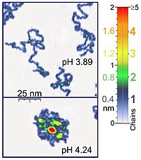
Another inconvenience is that an incorrect choice of tip for the required resolution can lead to image artifacts. Traditionally the AFM could not scan images as fast as an SEM, requiring several minutes for a typical scan, while an SEM is capable of scanning at near real-time (although at relatively low quality) after the chamber is evacuated. The relatively slow rate of scanning during AFM imaging often leads to thermal drift in the image (Lapshin, 2004, 2007), making the AFM microscope less suited for measuring accurate distances between artifacts on the image. However, several fast-acting designs were suggested to increase microscope scanning productivity (Lapshin and Obyedkov, 1993) including what is being termed videoAFM (reasonable quality images are being obtained with videoAFM at video rate - faster than the average SEM). To eliminate image distortions induced by thermodrift, several methods were also proposed (Lapshin, 2004, 2007).

AFM images can also be affected by hysteresis of the piezoelectric material (Lapshin, 1995) and cross-talk between the (x,y,z) axes that may require software enhancement and filtering. Such filtering could "flatten" out real topographical features. However, newer AFM use real-time correction software (for example, feature-oriented scanning, Lapshin, 2004, 2007) or closed-loop scanners which practically eliminate these problems. Some AFM also use separated orthogonal scanners (as opposed to a single tube) which also serve to eliminate cross-talk problems.

Due to the nature of AFM probes, they cannot normally measure steep walls or overhangs. Specially made cantilevers can be modulated sideways as well as up and down (as with dynamic contact and non-contact modes) to measure sidewalls, at the cost of more expensive cantilevers and additional artifacts.

歡迎來到Bewise Inc.的世界,首先恭喜您來到這接受新的資訊讓產業更有競爭力,我們是提供專業刀具製造商,應對客戶高品質的刀具需求,我們可以協助客戶滿足您對產業的不同要求,我們有能力達到非常卓越的客戶需求品質,這是現有相關技術無法比擬的,我們成功的滿足了各行各業的要求,包括:精密HSS DIN切削刀具協助客戶設計刀具流程DIN or JIS 鎢鋼切削刀具設計NAS986 NAS965 NAS897 NAS937orNAS907 航太切削刀具,NAS航太刀具設計超高硬度的切削刀具BW捨棄式鑽石V卡刀BW捨棄式金屬圓鋸片木工捨棄式金屬圓鋸片PCD木工圓鋸片醫療配件刀具設計汽車業刀具設計電子產業鑽石刀具全鎢鋼V卡刀-電路版專用全鎢鋼鋸片焊刃式側銑刀焊刃式千鳥側銑刀焊刃式T型銑刀焊刃式千鳥T型銑刀焊刃式螺旋機械鉸刀全鎢鋼斜邊刀電路版專用鎢鋼焊刃式高速鉸刀超微粒鎢鋼機械鉸刀超微粒鎢鋼定點鑽焊刃式帶柄角度銑刀焊刃式螺旋立銑刀焊刃式帶柄倒角銑刀焊刃式角度銑刀焊刃式筒型平面銑刀木工產業鑽石刀具等等。我們的產品涵蓋了從民生刀具到工業級的刀具設計;從微細刀具到大型刀具;從小型生產到大型量產;全自動整合;我們的技術可提供您連續生產的效能,我們整體的服務及卓越的技術,恭迎您親自體驗!!

BW Bewise Inc. Willy Chen willy@tool-tool.com bw@tool-tool.com www.tool-tool.com skype:willy_chen_bw mobile:0937-618-190 Head &Administration Office No.13,Shiang Shang 2nd St., West Chiu Taichung,Taiwan 40356 http://www.tool-tool..com / FAX:+886 4 2471 4839 N.Branch 5F,No.460,Fu Shin North Rd.,Taipei,Taiwan S.Branch No.24,Sec.1,Chia Pu East Rd.,Taipao City,Chiayi Hsien,Taiwan

Welcome to BW tool world! We are an experienced tool maker specialized in cutting tools. We focus on what you need and endeavor to research the best cutter to satisfy users demand. Our customers involve wide range of industries, like mold & die, aerospace, electronic, machinery, etc. We are professional expert in cutting field. We would like to solve every problem from you. Please feel free to contact us, its our pleasure to serve for you. BW product including: cutting toolaerospace tool .HSS DIN Cutting toolCarbide end millsCarbide cutting toolNAS Cutting toolNAS986 NAS965 NAS897 NAS937orNAS907 Cutting Tools,Carbide end milldisc milling cutter,Aerospace cutting toolhss drillФрезерыCarbide drillHigh speed steelMilling cutterCVDD(Chemical Vapor Deposition Diamond )’PCBN (Polycrystalline Cubic Boron Nitride) Core drillTapered end millsCVD Diamond Tools Inserts’PCD Edge-Beveling Cutter(Golden FingerEdge modifying knife

beeway 發表在 痞客邦 留言(0) 人氣()

Bewise Inc. www.tool-tool.com Reference source from the internet.
Image of reconstruction on a clean Gold(100) surface.

Image of reconstruction on a clean Gold(100) surface.

Scanning tunneling microscopy (STM) is a powerful technique for viewing surfaces at the atomic level. Its development in 1981 won its inventors, Gerd Binnig and Heinrich Rohrer (at IBM Zürich), the Nobel Prize in Physics in 1986[1]. STM probes the density of states of a material using tunneling current. For STM, good resolution is considered to be 0.1 nm lateral resolution and 0.01 nm depth resolution[2]. The STM can be used not only in ultra high vacuum but also in air and various other liquid or gas ambients, and at temperatures ranging from near 0 Kelvin to a few hundred degrees Celsius[3].

The STM is based on the concept of quantum tunneling. When a conducting tip is brought very near to a metallic or semiconducting surface, a bias between the two can allow electrons to tunnel through the vacuum between them. For low voltages, this tunneling current is a function of the local density of states (LDOS) at the Fermi level, Ef, of the sample[3]. Variations in current as the probe passes over the surface are translated into an image. STM can be a challenging technique, as it requires extremely clean surfaces and sharp tips.

[edit] Tunnelling

Tunnelling is a functioning concept that arises from quantum mechanics. Classically, an object hitting an impenetrable wall will bounce back. Imagine throwing a baseball to a friend on the other side of a mile high brick wall, directly at the wall. One would be rightfully astonished if, rather than bouncing back upon impact, the ball were to simply pass through to your friend on the other side of the wall. For objects of very small mass, as is the electron, wavelike nature has a more pronounced effect, so such an event, referred to as tunneling, has a much greater probability[3].

Electrons behave as waves of energy, and in the presence of a potential U(z), assuming 1-dimensional case, the energy levels ψn(z) of the electrons are given by solutions to Schrödinger’s equation,

- \frac{\hbar^2}{2m} \frac{\partial^2\psi_n (z)}{\partial z^2} + U(z) \psi_n (z) = E\psi_n (z) ,

where ħ is Planck’s constant, z is the position, and m is the mass of an electron[3]. If an electron of energy E is incident upon an energy barrier of height U(z), the electron wave function is a traveling wave solution,

\psi_n (z) = \psi_n (0)e^{\pm ikz},

where

 k=\frac{\sqrt{2m(E-U)}}{\hbar}

if E > U(z), which is true for a wave function inside the tip or inside the sample[3]. Inside a barrier, such as between tip and sample, E < U(z) so the wave functions which satisfies this are decaying waves,

\psi_n (z) = \psi_n (0)e^{\pm \kappa z},

where

 \kappa = \frac{\sqrt{2m(U-E)}}{\hbar}

quantifies the decay of the wave inside the barrier, with the barrier in the +z direction for − κ [3].

Knowing the wave function allows one to calculate the probability density for that electron to be found at some location. In the case of tunneling, the tip and sample wave functions overlap such that when under a bias, there is some finite probability to find the electron in the barrier region and even on the other side of the barrier[3]. Let us assume the bias is V and the barrier width is W, as illustrated in Figure 1. This probability, P, that an electron at z=0 (left edge of barrier) can be found at z=W (right edge of barrier) is proportional to the wave function squared,

P \propto |\psi_n (0)|^2 e^{-2 \kappa W} [3].

If the bias is small, we can let UEφM in the expression for κ, where φM, the work function, gives the minimum energy needed to bring an electron from an occupied level, the highest of which is at the Fermi level (for metals at T=0 kelvins), to vacuum level. When a small bias V is applied to the system, only electronic states very near the Fermi level, within eV, are excited[3]. These excited electrons can tunnel across the barrier. In other words, tunneling occurs mainly with electrons of energies near the Fermi level.

However, tunneling does require that there is an empty level of the same energy as the electron for the electron to tunnel into on the other side of the barrier. It is because of this restriction that the tunneling current can be related to the density of available or filled states in the sample. The current due to an applied voltage V (assume tunneling occurs sample to tip) depends on two factors: 1) the number of electrons between Ef and eV in the sample, and 2) the number among them which have corresponding free states to tunnel into on the other side of the barrier at the tip[3]. The higher density of available states the greater the tunneling current. When V is positive, electrons in the tip tunnel into empty states in the sample; for a negative bias, electrons tunnel out of occupied states in the sample into the tip[3].

Mathematically, this tunneling current is given by

 I \propto \sum_{E_f-eV}^{Ef} |\psi_n (0)|^2 e^{-2 \kappa W} .

One can sum the probability over energies between EfeV and eV to get the number of states available in this energy range per unit volume, thereby finding the local density of states (LDOS) near the Fermi level[3]. The LDOS near some energy E in an interval ε is given by

 \rho_s (z,E) = \frac{1}{\epsilon} \sum_{E- \epsilon}^{E} | \psi_n (z)|^2 ,

and the tunnel current at a small bias V is proportional to the LDOS near the Fermi level, which gives important information about the sample[3]. It is desirable to use LDOS to express the current because this value does not change as the volume changes, while probability density does[3]. Thus the tunneling current is given by

 I \propto V \rho_s (0, E_f) e^{-2 \kappa W}

where ρs(0,Ef) is the LDOS near the Fermi level of the sample at the sample surface[3]. By using equation (6), this current can also be expressed in terms of the LDOS near the Fermi level of the sample at the tip surface,

 I \propto V \rho_s (W, E_f) V

The exponential term in (9) is very significant in that small variations in W greatly influence the tunnel current. If the separation is decreased by 1 Ǻ, the current increases by an order of magnitude, and vice versa[4].

This approach fails to account for the rate at which electrons can pass the barrier. This rate should affect the tunnel current, so it can be accounted for by using Fermi’s Golden Rule with the appropriate tunneling matrix element. John Bardeen solved this problem in his study of the metal-insulator-metal junction, MIM[5]. He found that if he solved Schrödinger’s equation for each side of the junction separately to obtain the wave functions ψ and χ for each electrode, he could obtain the tunnel matrix, M, from the overlap of these two wave functions[3]. This can be applied to STM by making the electrodes the tip and sample, assigning ψ and χ as sample and tip wave functions, respectively, and evaluating M at some surface S between the metal electrodes at z=zo, where z=0 at the sample surface and z=W at the tip surface[3].

Now, Fermi’s Golden Rule gives the rate for electron transfer across the barrier, and is written

 w = \frac{2 \pi}{\hbar} |M|^2 \delta (E_{\psi} - E_{\chi} ) ,

where δ(Eψ-Eχ) restricts tunneling to occur only between electron levels with the same energy[3]. The tunnel matrix element, given by

 M= \frac{\hbar}{2 \pi} \int_{z=z_0} ( \chi* \frac {\partial \psi}{\partial z}-\psi \frac{\partial \chi*}{\partial z}) dS ,

is a description of the lower energy associated with the interaction of wave functions at the overlap, also called the resonance energy[3].

Summing over all the states gives the tunneling current as

 I = \frac{4 \pi e}{\hbar}\int_{-\infty}^{+\infty} [f(E_f -eV) - f(E_f + \epsilon)] \rho_s (E_f - eV + \epsilon) \rho_T (E_f + \epsilon)|M|^2 d \epsilon ,

where f is the Fermi function, ρs and ρT are the density of states in the sample and tip, respectively[3]. The Fermi distribution function describes the filling of electron levels at a given temperature T.

[edit] Procedure

First the tip is brought into close proximity of the sample by some coarse sample-to-tip control. The values for common sample-to-tip distance, W, range from about 4-7 Ǻ, which is the equilibrium position between attractive (3<10ǻ) id="cite_ref-Chen_2-20" class="reference">[3]. Once tunneling is established, piezoelectric transducers are implemented to move the tip in three directions. As the tip is rastered across the sample in the x-y plane, the density of states and therefore the tunnel current changes. This change in current with respect to position can be measured itself, or the height, z, of the tip corresponding to a constant current can be measured[3]. These two modes are called constant height mode and constant current mode, respectively.

In constant current mode, feedback electronics adjust the height by a voltage to the piezoelectric height control mechanism[6]. This leads to a height variation and thus the image comes from the tip topography across the sample and gives a constant charge density surface; this means contrast on the image is due to variations in charge density[4].

In constant height, the voltage and height are both held constant while the current changes to keep the voltage from changing; this leads to an image made of current changes over the surface, which can be related to charge density[4]. The benefit to using a constant height mode is that it is faster, as the piezoelectric movements require more time to register the change in constant current mode than the voltage response in constant height mode[4].

In addition to scanning across the sample, information on the electronic structure of the sample can be obtained by sweeping voltage and measuring current at a specific location[2]. This type of measurement is called scanning tunneling spectroscopy (STS).

[edit] Instrumentation

Schematic view of an STM

Schematic view of an STM

The components of an STM include scanning tip, piezoelectric controlled height and x,y scanner, coarse sample-to-tip control, vibration isolation system, and computer[6].

The resolution of an image is limited by the radius of curvature of the scanning tip of the STM. Additionally, image artifacts can occur if the tip has two tips at the end rather than a single atom; this leads to “double-tip imaging,” a situation in which both tips contribute to the tunneling[2]. Therefore it has been essential to develop processes for consistently obtaining sharp, usable tips. Recently, carbon nanotubes have been used in this instance.

A closeup of a simple scanning tunneling microscope head at the University of St Andrews scanning MoS2 using a Platinum-Iridium stylus.

A closeup of a simple scanning tunneling microscope head at the University of St Andrews scanning MoS2 using a Platinum-Iridium stylus.

The tip is often made of tungsten or platinum-iridium, though gold is also used[2]. Tungsten tips are usually made by electrochemical etching, and platinum-iridium tips by mechanical shearing[2]. Both processes are outlined in C. Bai’s book, reference[2] below.

Due to the extreme sensitivity of tunnel current to height, proper vibration isolation is imperative for obtaining usable results. In the first STM by Binnig and Rohrer, magnetic levitation was used to keep the STM free from vibrations; now spring systems are often used[3]. Additionally, mechanisms for reducing eddy currents are implemented.

Maintaining the tip position with respect to the sample, scanning the sample in raster fashion and acquiring the data is computer controlled[6]. The computer is also used for enhancing the image with the help of image processing as well as performing quantitative morphological measurements.

[edit] Other STM Related Studies

Many other microscopy techniques have been developed based upon STM. These include Photon Scanning Tunneling Microscopy (PSTM), which uses an optical tip to tunnel photons[2]; Scanning Tunneling Potentiometry (STP), which measures electric potential across a surface[2]; and spin polarized scanning tunneling microscopy (SPSTM), which uses a ferromagnetic tip to tunnel spin-polarized electrons into a magnetic sample[7].

Other STM methods involve manipulating the tip in order to change the topography of the sample. This is attractive for several reasons. Firstly the STM has an atomically precise positioning system which allows very accurate atomic scale manipulation. Furthermore, after the surface is modified by the tip, it is a simple matter to then image with the same tip, without changing the instrument. IBM researchers developed a way to manipulate Xenon atoms absorbed on a nickel surface[2] This technique has been used to create electron "corrals" with a small number of adsorbed atoms, which allows the STM to be used to observe electron Friedel Oscillations on the surface of the material. Aside from modifying the actual sample surface, one can also use the STM to tunnel electrons into a layer of E-Beam photoresist on a sample, in order to do lithography. This has the advantage of offering more control of the exposure than traditional Electron beam lithography.

Recently groups have found they can use the STM tip to rotate individual bonds within single molecules. The electrical resistance of the molecule depends on the orientation of the bond, so the molecule effectively becomes a molecular switch.

[edit] Early Invention

An early, patented invention, based on the above-mentioned principles, and later acknowledged by the Nobel committee itself, was the Topografiner of R. Young, J. Ward, and F. Scire from the NIST ("National Institute of Science and Technolology" of the USA)[8].

歡迎來到Bewise Inc.的世界,首先恭喜您來到這接受新的資訊讓產業更有競爭力,我們是提供專業刀具製造商,應對客戶高品質的刀具需求,我們可以協助客戶滿足您對產業的不同要求,我們有能力達到非常卓越的客戶需求品質,這是現有相關技術無法比擬的,我們成功的滿足了各行各業的要求,包括:精密HSS DIN切削刀具協助客戶設計刀具流程DIN or JIS 鎢鋼切削刀具設計NAS986 NAS965 NAS897 NAS937orNAS907 航太切削刀具,NAS航太刀具設計超高硬度的切削刀具BW捨棄式鑽石V卡刀BW捨棄式金屬圓鋸片木工捨棄式金屬圓鋸片PCD木工圓鋸片醫療配件刀具設計汽車業刀具設計電子產業鑽石刀具全鎢鋼V卡刀-電路版專用全鎢鋼鋸片焊刃式側銑刀焊刃式千鳥側銑刀焊刃式T型銑刀焊刃式千鳥T型銑刀焊刃式螺旋機械鉸刀全鎢鋼斜邊刀電路版專用鎢鋼焊刃式高速鉸刀超微粒鎢鋼機械鉸刀超微粒鎢鋼定點鑽焊刃式帶柄角度銑刀焊刃式螺旋立銑刀焊刃式帶柄倒角銑刀焊刃式角度銑刀焊刃式筒型平面銑刀木工產業鑽石刀具等等。我們的產品涵蓋了從民生刀具到工業級的刀具設計;從微細刀具到大型刀具;從小型生產到大型量產;全自動整合;我們的技術可提供您連續生產的效能,我們整體的服務及卓越的技術,恭迎您親自體驗!!

BW Bewise Inc. Willy Chen willy@tool-tool.com bw@tool-tool.com www.tool-tool.com skype:willy_chen_bw mobile:0937-618-190 Head &Administration Office No.13,Shiang Shang 2nd St., West Chiu Taichung,Taiwan 40356 http://www.tool-tool..com / FAX:+886 4 2471 4839 N.Branch 5F,No.460,Fu Shin North Rd.,Taipei,Taiwan S.Branch No.24,Sec.1,Chia Pu East Rd.,Taipao City,Chiayi Hsien,Taiwan

Welcome to BW tool world! We are an experienced tool maker specialized in cutting tools. We focus on what you need and endeavor to research the best cutter to satisfy users demand. Our customers involve wide range of industries, like mold & die, aerospace, electronic, machinery, etc. We are professional expert in cutting field. We would like to solve every problem from you. Please feel free to contact us, its our pleasure to serve for you. BW product including: cutting toolaerospace tool .HSS DIN Cutting toolCarbide end millsCarbide cutting toolNAS Cutting toolNAS986 NAS965 NAS897 NAS937orNAS907 Cutting Tools,Carbide end milldisc milling cutter,Aerospace cutting toolhss drillФрезерыCarbide drillHigh speed steelMilling cutterCVDD(Chemical Vapor Deposition Diamond )’PCBN (Polycrystalline Cubic Boron Nitride) Core drillTapered end millsCVD Diamond Tools Inserts’PCD Edge-Beveling Cutter(Golden FingerEdge modifying knifeSolid carbide saw blade-V typeV-type locking-special use for PC boardMetal Slitting SawaCarbide Side milling CuttersCarbide Side Milling Cutters With Staggered TeethCarbide T-Slot Milling CuttersCarbide T-Slot Milling Cutters With Staggered TeethCarbide Machine Reamers

beeway 發表在 痞客邦 留言(0) 人氣()